Author: Godot
Our story begins with a competition.
Fei-Fei Li, former Vice President of Google and Chief Scientist of Google Cloud AI/ML, also a professor at Stanford University. But she has another identity—founder of the ImageNet competition.
The ImageNet competition, formally known as ILSVRC (ImageNet Large Scale Visual Recognition Challenge), is the most influential academic competition in the field of computer vision.
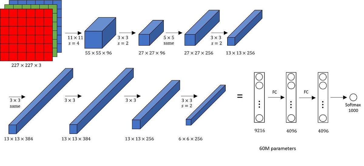
In the 2012 ImageNet competition, Geoffrey Hinton’s student Alex Krizhevsky shocked the world by lowering the image recognition error rate from 26% to 15.3% with his AlexNet neural network, leading the second place by an astonishing 10.8 percentage points.
The key point is that AlexNet did not use supercomputers, but solely relied on two ordinary NVIDIA GTX 580 gaming graphics cards to complete the training. This marked AI's first large-scale use of GPU acceleration. Before this, training primarily relied on CPUs.
This result announced to the world: AI deep learning + GPU = computational power revolution.
As researchers turned their attention to GPUs, they discovered that only NVIDIA’s CUDA allowed them to write complex algorithms in C-like languages.
Jensen Huang's "Ten-Year Gamble"
Time rewinds to 2006. At that time, the only responsibility of GPUs was to render game graphics.
But Jensen Huang wanted GPUs to become general computing tools. He firmly believed that Moore's Law was nearing its end for CPUs, and the future of serial computing would inevitably be parallel computing.
So in 2006, Chief Scientist Ian Buck led the development of CUDA (Compute Unified Device Architecture). However, at that time, no one knew what this thing was for.
To support CUDA, NVIDIA embedded an additional specialized computing circuit in every GPU chip. This meant larger chip size, higher power consumption, reduced yield, and skyrocketing costs.
Except for a few researchers, no one bought it. Before the deep learning boom, NVIDIA even proactively sent graphics cards for free to top laboratories around the world, along with engineers to assist in optimization.
CUDA burned about $500 million of NVIDIA's R&D expenses each year, while the company's annual profit was only a few hundred million dollars. When the financial crisis hit in 2008, NVIDIA's stock price plummeted.
Jensen Huang, under the pressure of falling stock prices, persisted for a full ten years. He always believed that GPUs were not just for rendering game graphics but were general-purpose parallel processors.
At the turning point in 2012, Intel was still busy maintaining CPU hegemony. Intel had long been superstitious about the generality of CPUs, believing that neural networks were just a passing trend. Even if it needed computation, it could be solved by extending the CPU instruction set (like AVX).
At that time, AMD was deeply mired in post-acquisition pain, very stingy with software investment, leading to its AI software stack ROCm lagging behind CUDA significantly in usability and stability even today.
Thus, in the summer of 2012, Alex Krizhevsky faced millions of images in the ImageNet competition and was worried that CPUs could not handle the computation. He found CUDA extremely useful, writing thousands of lines of code in a C-like language and running it on two GTX 580 graphics cards.
The result shocked the global academic community. An experiment that originally would take several weeks to run produced results in just a few days on GPUs, with accuracy leading by a considerable margin.
Abandoning Mobile Internet, Fully Turning to GPU Computing
In 2013, Jensen Huang made a decision that seemed almost insane at the time, shifting the company's focus entirely to GPU computing.
That was the golden age of mobile internet, with the smartphone wave in full swing. Although NVIDIA faced setbacks in the mobile market, it did not stubbornly engage in the mobile chip sector, but decisively withdrew all resources back and bet on the then highly niche data center accelerated computing.
In the same year, CUDA entered the 5.0/5.5 era, introducing dynamic parallelism, allowing GPUs to start new tasks on their own without going back to the CPU, significantly reducing communication delay.
At the same time, NVIDIA secretly started developing cuDNN internally, a CUDA deep learning library specifically designed for deep neural networks, encapsulating the most difficult convolution algorithms in neural networks directly in the underlying library. Developers could complete operations with just a single command.
On the other hand, for AMD’s graphics cards, the same functions required hundreds of lines of complex low-level code to be written by the user.
In 2014, the deep learning framework melee began. Google open-sourced TensorFlow, prompting NVIDIA to send many engineers to the open-source community to continuously optimize CUDA adaptation. When TensorFlow 1.0 was released, its running efficiency on NVIDIA graphics cards was several times higher than on AMD graphics cards.
“Buy NVIDIA graphics cards” began to become an industry consensus.
To this day, CUDA has evolved from a development tool into an industry standard language. Hundreds of millions of AI code repositories on GitHub rely on CUDA primitives, and nearly all university courses teach based on CUDA. This means the next generation of engineers becomes "natives" of the NVIDIA ecosystem before graduation.
Hundreds of millions of AI code repositories on GitHub rely on CUDA primitives. University courses are almost entirely based on CUDA teaching. This means the next generation of engineers has already become "natives" of the NVIDIA ecosystem before graduation.
Above CUDA, there is also a large middleware and library system.
A. cuDNN and cuBLAS
Deep neural networks and linear algebra libraries have undergone over a decade of hand-assembly optimization.
B. TensorRT
Inference optimization engine that can automatically fuse operators, select the best kernel, and perform quantization calibration. After entering the Blackwell era, TensorRT-LLM became the standard for deploying large language models, directly supporting extreme optimizations like FP4/FP8, making it hard for competitors to catch up.
C. Triton Inference Server
Has become the de facto standard for cloud-native AI inference.
Jensen Huang, Musk, OpenAI, “Attention is All You Need”… In 2017, AI Deity Emerges
In 2017, NVIDIA's Volta architecture was born, followed closely by the release of the flagship Tesla V100. This chip introduced the Tensor Core for the first time.
AI computation shifted from the era of vector operations to matrix operations at this moment. AI computational power exploded, heralding the beginning of the new era.
Earlier, at the end of 2016, Jensen Huang personally delivered the world’s first DGX-1 supercomputer equipped with early accelerator cards to the then little-known OpenAI office.
Thus came that famous photo. The person crossing his arms in the photo is indeed the financier of OpenAI, Musk. This machine later became the "ancestor machine" for training the GPT series models.
In 2017, another seemingly unrelated but actually decisive event occurred: Google published the paper "Attention is All You Need," proposing the Transformer architecture.
This paper laid the cornerstone for today’s large language models, completely changing the way AI processes information, and directly contributing to the later emergence of ChatGPT, Claude, Gemini, and other large models.
The computation of the Transformer architecture consists almost entirely of matrix multiplication, making its demand for computational power extremely greedy.
Matrix multiplication, does that ring a bell? That's right, NVIDIA's Tensor Core was born specifically for matrix multiplication.
At this point, the "Cambrian explosion" of AI officially began.
From a macro perspective, NVIDIA's dominance is built on three pillars:
1) Tensor Core architecture
Realizes the leap from vector computing to matrix computing and from general computing to deep learning-specific computing.
2) CUDA software ecosystem
NVIDIA's deepest moat, not just a programming language, but also a huge collection of libraries and tools including cuDNN and cuBLAS, making the cost of migration extremely high.
3) NVLink interconnect technology
The bridge for collaboration between GPUs.
To simplify the relationship among the three: Tensor Core is hardware innovation, CUDA is the software ecosystem, and NVLink is the interconnection channel, corresponding to performance, ecosystem, and composability respectively.
Tensor Core is the key that truly puts NVIDIA ahead of its competitors and establishes its dominant position in AI. Without understanding Tensor Core, one cannot understand modern AI chips.
Tensor Core marks the thorough transformation of GPUs from graphics rendering devices to AI-specific computing platforms, sacrificing generality to achieve extreme performance in matrix multiplication, the core operation of AI.
What is Tensor Core?
Tensor Core can be further broken down into three core concepts:
1) Matrix multiplication 2) Mixed precision 3) Architectural evolution
1) Matrix multiplication
The transition from vector computation to matrix computation is the core logic behind Tensor Core's leap in performance.
Traditional CUDA Cores perform scalar or vector operations, such as A + B. Even when executed concurrently, each cycle can only process a limited number of data points.
Tensor Cores, on the other hand, are embedded DSA (Domain-Specific Architecture) modules within the GPU. They essentially incorporate ASIC-level dedicated acceleration units within the general GPU architecture.
Tensor Cores are not meant to execute all types of instructions but instead specialize in a specific operation—matrix multiply-accumulate, i.e., D = A × B + C.
Simply put, vector computation is like issuing computation commands line by line; matrix computation directly outputs an entire block of data (4×4 matrix).
2) Mixed precision—The art of fuzziness
The essence of AI is probability, not certainty.
Determining whether an image is of a cat or a dog, a probability of 98.0001% is not significantly different from 98.0000000001% probability. However, the difference in precision greatly impacts computational efficiency.
Mixed precision means using lower precision as much as possible without affecting result correctness to achieve extreme efficiency.
A. How to measure precision?
Here we introduce a concept: FP (Floating Point), which refers to floating-point numbers.
Internally in a computer, any number is composed of 0s and 1s (bits). A floating-point number typically contains three parts:
1) Sign bit, indicating whether the number is positive or negative. 2) Exponent, determining the range of the number. 3) Mantissa/Fraction, determining the precision of the number, i.e., how many digits are there after the decimal point.
Commonly used formats like FP32 record a number in 32 bits, being highly accurate but occupying a large space.
FP16 halves the space and doubles the speed, but its precision and range shrink accordingly; FP4 offers extremely low precision, resembling pixel art, capable of only recording very vague values.
In computer science, this essentially seeks an optimal solution between effective information volume (information entropy), computing throughput, and numerical stability.
B. How does mixed precision work?
a. Precision degradation
During computation, Tensor Core forces the originally 32-bit input to convert to 16 bits.
FP32: 1 bit sign + 8 bits exponent + 23 bits mantissa. FP16: 1 bit sign + 5 bits exponent + 10 bits mantissa.
The mantissa dimension drops from 23 to 10, and during the matrix multiplication stage, the computational pressure decreases by more than 4 times.
b. Accumulate protection
This is the most ingenious aspect of Tensor Core's design.
The input is FP16, but accumulation uses FP32—note that addition uses FP32.
This is because small errors while multiplying are typically safe, but in tens of thousands of additions, continuously discarding small values amplifies errors quickly. Accumulating at high precision ensures the accuracy of the final results for NVIDIA.
c. Loss scaling—Counteracting "underflow"
In AI training, using FP16 throughout can cause the model to collapse. Some key data might be extremely small, which FP16 cannot express, a problem termed underflow.
The countermeasure is for the program to multiply the loss value by a huge coefficient (like 1024) before calculation, forcing these small gradients back into the effective range expressible by FP16. After computation, it divides by 1024 to restore.
C. Limits of mixed precision—Microscaling Format (MX) micro-scaling
NVIDIA V100 supports FP16, but by the time of H100, it has turned to FP8, and B200 further reduces it to FP4.
Although FP4 is remarkably faster than FP16, it can only express 2⁴ = 16 numerical values. It’s important to understand that a single image contains far more than 16 colors; AI would be unable to distinguish Van Gogh's "Sunflowers" from "Starry Night."
Thus, in the Blackwell architecture, NVIDIA introduced Microscaling Format, whose core idea is block floating-point (Block Floating Point).
Simply put, within the same vector block of an AI network, the magnitudes of numerical values are often similar. Rather than scaling each value individually, it's more efficient to process in batches: find the value with the absolute largest magnitude in a batch to determine a common scaling factor.
The most challenging scenario is when a dataset contains one extremely large number, and the rest are very small values.
It’s like a photo containing both the sun and a faint firefly nearby. Such "anomalous values" frequently occur in certain layers of AI Transformers.
This is precisely why NVIDIA did not entirely discard FP8 and FP16 in the Blackwell architecture and instead invested significant effort in software-level smoothing.
3) Architectural evolution
Here’s a convenient way to remember:
Volta was born—Ampere went mainstream—Hopper exploded—Blackwell is the hottest now.
The later the year, the later the architecture name, the smaller the supported precision (the number after FP), the larger the scale of matrix operations, and the more AI resembles human-like behavior.
In 2017, Volta (V100): An extremely risky gamble
The birth of Volta in 2017 marked a critical watershed in NVIDIA's development.
Before this, the Pascal architecture, such as GTX 1080 Ti, primarily aimed to enhance the visual appeal of games.
Starting with Volta, Jensen Huang made an extremely risky yet retrospectively brilliant decision—to adopt mixed precision, thus reducing precision for extreme AI computing efficiency, transforming GPUs from general computing devices into AI-specific platforms.
Before 2017, the scientific computing domain, such as weather simulations and nuclear explosion simulations, demanded absolute precision, leading everyone to chase FP32 single precision or even FP64 double precision computing power.
But then suddenly, AI exploded. And AI networks are particularly "noise-resistant."
Training AI is akin to teaching a child to recognize a cat; there's no need to tell the child that this cat has ears measuring 3.1415926 centimeters long; just saying it's about 3 centimeters is sufficient.
NVIDIA vigorously promoted mixed precision on the V100: using FP16 for computations and FP32 for accumulation to prevent error accumulation. This is akin to transforming from writing in standard script to cursive, doubling the speed while AI accuracy saw virtually no decline.
This was extraordinarily risky at the time. Allocating a large area in an extremely expensive chip for dedicated circuitry to support matrix operations, which was used by only a limited number of people then, was a very, very, very risky decision.
Yet Huang and NVIDIA bet on the explosion of AI.
As a result, this became the reason why other competitors, such as Intel, are still lagging behind today.
2018 Turing (T4)—A Super Revolution in Game Graphics: Ray Tracing and DLSS
By this time, the main use case of chips remained game graphics rendering.
In 2018, NVIDIA released the Turing architecture (RTX 2080 Ti). This was the first time in graphics card history that three completely different types of processors were encapsulated on the same silicon chip.
Let’s clarify the background.
Previously, game graphics rendering utilized rasterization, essentially 2D texture mapping. Experienced gamers should be very familiar with this. For example, the reflection on water isn't dynamically calculated but is pre-drawn and pasted; when the player's perspective shifts, the shadow remains static.
Ray tracing simulates the physical light and shadow effects of the real world. In games, light and reflections shift in real-time with the player's perspective and light source.
Ray tracing was not impossible before; it just required immense computation, causing games to lag significantly.
In the Turing architecture, the three completely different types of processors include RT Core, CUDA Core, and Tensor Core.
1) RT Core (Ray Tracing Core)
This is a Turing innovation dedicated to calculating the intersection between rays and triangles (BVH Traversal). Its function is extremely specific: it only handles ray tracing calculations, dramatically enhancing efficiency by separating such tedious geometric calculations from general cores.
2) CUDA Core (General Purpose Computing Core)
It continues to take on traditional rasterization rendering tasks.
3) Tensor Core (Mixed Precision Computing Core)
It added support for INT8, INT4, and INT1, introducing low precision inference capabilities and bringing Tensor Core to consumer-grade graphics cards (RTX 20 series) for the first time.
Here lies a significant invention—DLSS (Deep Learning Super Sampling).
The logic is that ray tracing computation is too demanding, so first rendering a 1080P image and then using Tensor Core to run a neural network to "imagine" the 1080P image into 4K.
This marked the first large-scale application of AI-generated content in the graphics realm, proving that AI could become part of the traditional graphics pipeline.
By around 2018, traditional performance growth had hit a ceiling. NVIDIA's strong push for ray tracing fundamentally redefined the standard of measuring the quality of graphics cards. Even if AMD or Intel wanted to catch up, they lacked efficient hardware like Tensor Core to support it.
In other words, NVIDIA created a comprehensive blockade of "algorithms + hardware + training data."
The combination of ray tracing and Tensor Core also unexpectedly opened the door to the metaverse and digital twins.
If Tensor Core can complete game graphics through AI, could it generate a real 3D space based on a few photos? This is the trendy NeRF neural radiance field technology in recent years, achieving 3D modeling from videos in just seconds.
2020 Ampere (A100)—The Most Successful AI Chip in History
Describing the A100 as a "revolution in usability" couldn't be more fitting. Before A100, there were three problems in the computational field: 1) Precision fragmentation. FP32 is too slow, FP16 is too difficult to handle; 2) Computational power fragmentation. Training cards and inference cards are not interchangeable; 3) Resource fragmentation. Large models can't get enough power, while small models are overloaded.
NVIDIA made groundbreaking improvements with the A100: 1) TF32 (TensorFloat-32) 2) Structured Sparsity 3) MIG (Multi-Instance GPU)
These three collectively achieved unification for a single chip.
TensorFloat-32 (TF32)
This is a genius design. Remember earlier when we mentioned that prior AI computations adhered to high precision solutions, conducting weather simulations, particle simulations, and nuclear explosion trajectory predictions?
TF32 allows developers who are accustomed to writing high-precision FP32 code to directly enjoy Tensor Core’s fuzzy precision acceleration without changing their code.
TF32 is not a completely new storage format but a computational intermediate format.
It achieves acceleration by "truncating" FP32, essentially balancing computational precision with numerical range and creating a new mathematical format.
Previously, we noted that within a computer, any number consists of 0s and 1s (bits). A floating-point number typically consists of three parts: 1) Sign bit, indicating whether the number is positive or negative. 2) Exponent, determining the size range of the number. 3) Mantissa/Fraction, determining the precision of the number, i.e., how many decimal places it contains.
Common formats like FP32 record numbers in 32 bits, extremely precise but large in space; FP16 halves the space and doubles the speed but reduces both precision and range; FP4 represents a very low precision, resembling pixel art, only able to capture very vague values.
The brilliance of TF32 lies in its ability to combine the range of FP32 with the precision of FP16 to form a 19-bit format: 1 bit sign, 8 bits exponent (same as FP32), and 10 bits mantissa (same as FP16).
In other words, TF32 serves as a bridge between FP32 and FP16. Isn’t that genius!!!!!!!!
Its workflow is as follows: TF32 reads standard FP32 data from memory, and the Tensor Core automatically truncates the mantissa from 23 bits to 10 bits within the hardware circuitry, executing efficient multiplication in this format; all intermediate products are eventually accumulated at FP32 precision; the data written back to memory remains standard FP32.
More crucially, the truncation process is entirely automatic, meaning it can effectively address potential underflow issues.
Structured Sparsity
Sparsity fundamentally means turning unimportant weights to 0. For example, when recognizing an image of a cat, most pixels do not play a decisive role.
NVIDIA mandates that among every 4 consecutive weights, at least 2 must be set to 0. Data that originally required 64 bits now only needs about 34 bits, effectively halving the model's memory footprint.
For instance, if a graphics card has 80GB of memory, it could originally accommodate a model with 40 billion parameters. With structured sparsity enabled, it might fit a model with nearly 70 billion or even 80 billion parameters.
Moreover, performance could double. Dense computation achieves 156 TFLOPS (156 trillion operations per second), while sparse computation hits 312 TFLOPS.
If we further add on the nearly 10-fold improvement that TF32 brings compared to traditional FP32, it is evident that A100 processes specific AI tasks faster than older graphics cards from a few years ago by an entire era.
As for whether there’s concern that all four weights are crucial, resulting in the loss of key information? Firstly, when a model is not yet "fixed," weights can still be fluidly adjusted.
Secondly, neural networks possess exceptional fault tolerance—though some information may be lost in a small local area, other layers can learn to compensate for that loss.
Additionally, sparsity is not about randomly deleting but is instead based on pruning weights by significance.
MIG (Multi-Instance GPU)
MIG is used for chip space management, physically "hard partitioning" a single GPU at the physical circuit level. Not mistaken, it’s a physical layer segmentation.
On the A100, MIG can partition the GPU into a maximum of 7 independent instances (Instances), each having its own dedicated Tensor Core and memory pathway.
The segmentation method is flexible, e.g., cutting into 7 small instances, or 1 large instance with 3 small ones. The hardware comes pre-equipped with this "cutting" capability, but how and into how many parts it’s segmented can be controlled in real-time via software commands after purchase.
In the hardware structure of the A100, MIG primarily segments three core resources: 1) SM (Streaming Multiprocessor). The computation core, including CUDA Core and Tensor Core. 2) Memory system, comprising HBM2 memory and L2 cache. 3) Bandwidth (Pathways), the data transmission channels within the chip (On-chip crossbar).
Each instance has its independ
免责声明:本文章仅代表作者个人观点,不代表本平台的立场和观点。本文章仅供信息分享,不构成对任何人的任何投资建议。用户与作者之间的任何争议,与本平台无关。如网页中刊载的文章或图片涉及侵权,请提供相关的权利证明和身份证明发送邮件到support@aicoin.com,本平台相关工作人员将会进行核查。


