Author: Duqin DQ
Previously, we analyzed in depth the lamentable low period of this flash memory giant: burdened by the former glory of Toshiba Storage yet “out of sync with the times”; facing cold eyes from the capital market, leading to IPO setbacks; suffering massive losses during the industry's winter, and unfortunately missing out on the tremendous fortune of HBM, even the alliance with Western Digital ended in failure… At that time, Kioxia seemed to outsiders to have become a “hot potato” in the reshuffling of the semiconductor industry.
However, just over a year later, Kioxia staged what can be described as an epic comeback. Driven madly by AI large models, the market logic of storage underwent a fundamental reversal, and Kioxia not only succeeded in a comeback but also achieved a dual explosion in the capital market and technology.
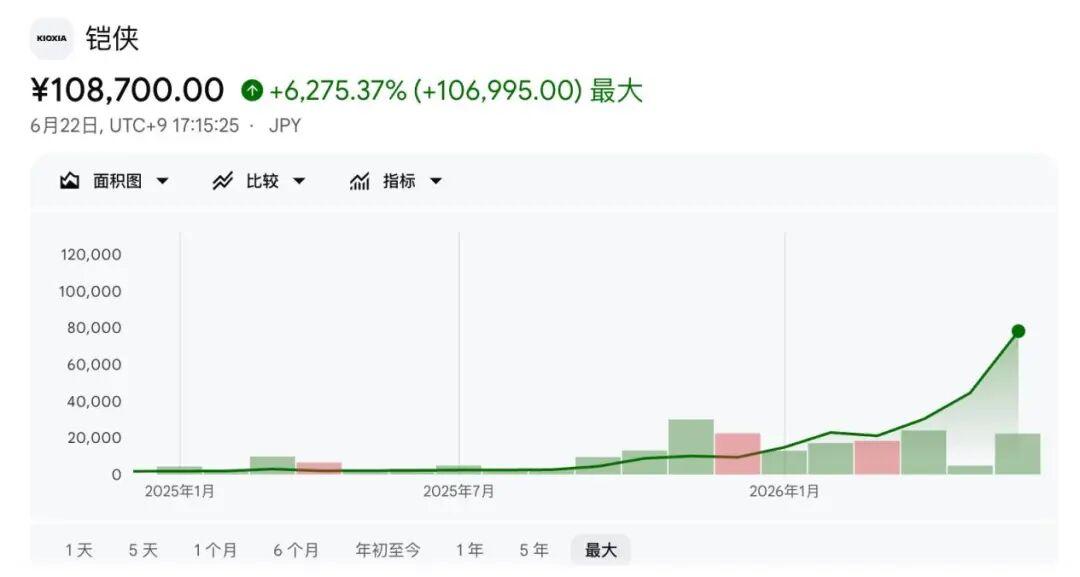
Kioxia’s stock price trend since its listing
The Super Myth of the Capital Market
Kioxia successfully listed on the Tokyo Stock Exchange at the end of 2024, with an initial market value hovering around 800 billion yen (approximately 5 billion USD). However, following the explosive demand for AI storage, Kioxia staged an epic resurgence within 18 months post-listing: its stock price skyrocketed over 50 times in 18 months, and rose 8 times in just the year 2026.
Currently, Kioxia's market value has surpassed 51 trillion yen (approximately 481 trillion KRW), repeatedly surpassing Toyota, the symbol of Japanese manufacturing, to become the company with the highest market value on the Japanese stock market.
According to Kioxia's performance forecast for the first quarter of the fiscal year 2026 (April–June), its single-quarter operating profit is expected to reach 1.3 trillion yen (approximately 81 billion USD), a nearly 30-fold year-on-year increase; the single-quarter net profit forecast is 869 billion yen, an increase of 48 times year-on-year, with just one quarter's performance exceeding the annual net profit forecast for the fiscal year 2025.
As major customers rush to sign long-term supply contracts, Kioxia's NAND capacity for 2026 has been sold out, and the supply-demand imbalance is expected to continue into 2027. The market expects Kioxia's operating profit margin this year to exceed 60%, setting a record for the highest profitability level in the global memory industry. Furthermore, with the market anticipating that shareholders will receive stock splits and dividends, its target stock price is expected to rise to 200,000 yen.
This surge has allowed its parent company Bain Capital, which held firm during the low period, and the indirect major shareholder SK Hynix, to achieve unimaginable investment returns.
According to the Financial Times, the AI boom has made Bain's acquisition of Toshiba Storage (now Kioxia) in 2018 one of the most profitable private equity deals in history. Bain Capital has already realized profits by selling off most of its shares, with returns exceeding 15 billion USD, and a return rate nearing 20 times; its flagship private equity fund is estimated to have gained over 8 billion USD in profits.
SK Hynix invested a total of 395 billion yen (approximately 3.9 trillion KRW at the time) in Toshiba Storage through a Korea-U.S.-Japan consortium in 2018. Currently, this consortium still holds an 18% stake in Kioxia. With Kioxia's stock price soaring, SK Hynix is realizing massive paper gains, and the market anticipates that the total profit obtained by this consortium will far exceed 70 billion USD.
What was once a “hot potato” has instantly transformed into a “super ATM.”
In the past, the dividends of artificial intelligence primarily concentrated on GPU and HBM companies like Nvidia and SK Hynix. HBM is the star on the AI training side, while NAND has become a scarce resource in AI inference, model storage, data lakes, enterprise-level SSDs, and nearline storage. The market anticipates that Kioxia's net profit for the fiscal year 2027 will reach 28.389 trillion yen, a 5.1-fold increase compared to the previous year.
3D NAND, Kioxia's Fundamental Lifeline
Kioxia invented NAND flash memory over 35 years ago, and in 2007, Kioxia launched BiCS FLASH 3D flash memory, a technical system centered around vertical stacking, horizontal scaling, wafer bonding, select gate optimization, and advanced packaging.
The fundamental idea of 3D NAND is: unlike 2D NAND, it no longer just reduces the unit size in a plane, but instead stacks memory cells vertically like building a tall building. Kioxia’s explanation is vivid: it was originally one floor, and there was limited land area; 3D NAND is like turning one floor into a multi-story apartment, accommodating more “tenants” in the same area.
The core of BiCS FLASH lies in its batch processing technology. Its general processing logic is: first alternately stack planar electrodes and insulating layers; then create a large number of holes in a single step along the vertical direction; then fill the holes with charge storage films and columnar electrodes; the intersection of the planar electrodes and columnar electrodes forms a memory cell. This shows that Kioxia's BiCS FLASH does not involve “individually making a memory cell every time a layer is added” in the traditional sense, but first stacks structures, then forms memory cells across multiple layers in one go through a “punch and plug” method. Therefore, as the number of layers increases, manufacturing costs do not rise completely linearly, thus improving the economic viability of continuing to stack 3D NAND.
Kioxia has disclosed that the commercialization rhythm of BiCS FLASH is roughly as follows: BiCS FLASH products achieved 48 layers of commercialization in 2015, then progressed to 96 layers, 112 layers, and 162 layers; as of March 2023, over 200 layers of stacking had been achieved.
Among these, the 8th generation of BiCS FLASH is a critical node. Kioxia states that the 8th generation products employ 218 word-line stacks, achieving a 1Tb TLC product storage density of 18.3Gb/mm², and supporting an external data transfer speed of 3.2Gbps, a 40μs read time, and 205MB/s programming throughput.
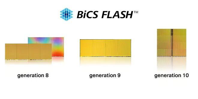
Kioxia's 8th generation BiCS FLASH not only jumped from 162 layers to 218 layers but also introduced two key technologies:
CBA (CMOS directly Bonded to Array): CBA can be understood as manufacturing the peripheral CMOS control circuit and memory array separately, then performing wafer bonding. In the past, CMOS circuits and memory arrays were manufactured on the same wafer. However, the optimal processing conditions required for both are not entirely the same: memory arrays may need processes more suited to charge storage and stacking structures, while CMOS circuits focus more on logical control, electrical performance, and speed. Putting both on the same wafer leads to mutual compromise.
The approach of CBA is: manufacturing CMOS wafers separately and memory array wafers separately, optimizing the processes individually, and finally bonding them together with high precision. The benefits brought by this are: enhanced bit density, increased NAND I/O speed, enabling the memory array to adopt high-temperature processes that were previously challenging due to CMOS constraints, and reducing electrical interference between adjacent memory cells.
OPS (On Pitch Select Gate): OPS addresses the issue of space waste within the memory array. In traditional structures, there exist some “dummy” areas between memory cells that do not store data. These areas do not directly contribute to capacity but occupy space. Kioxia's OPS technology reduces or eliminates these ineffective areas by rearranging the select gate and isolation structure, allowing for more effective memory cells to fit in the same area. Kioxia explains that OPS removes unnecessary dummy areas, allowing for more actual memory cells to be placed in the same space, thereby significantly enhancing storage density.
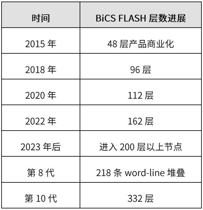
The 9th generation BiCS FLASH mainly targets 512Gb and 1Tb TLC products, aiming to support high-performance and low-power applications in the mid-low capacity range. It continues to use CBA and OPS technology to improve production efficiency and provide more advanced flash memory solutions. The 9th generation does not adopt the route of increasing layers but emphasizes the balance of performance, power consumption, cost, and production efficiency.
The 10th generation BiCS FLASH, on the other hand, is clearly more focused on future high-capacity and high-performance needs. Kioxia indicates that the 10th generation products adopt the same CMOS technology as the 9th generation while increasing the number of storage layers to 332 layers, approximately 1.5 times that of the 8th generation, to enhance bit density and power efficiency.
In addition to upstream processing, Kioxia is also enhancing its back-end packaging capabilities. Official materials mention that Kioxia has developed an 8TB flash memory in a single package by stacking 32 chips of 2Tb flash dies within one package. This relies on advanced back-end processes such as wafer thinning, material design, and wire bonding. This 32-die stacking can assemble 32 2Tb dies into a package with a height of less than 2mm, forming an 8TB flash memory solution.
From 3D NAND to 3D DRAM, Kioxia’s New Gamble
Kioxia is also breaking down the barriers of being a “pure NAND manufacturer” with a secret weapon. So why is Kioxia venturing into 3D DRAM? This is because DRAM has also encountered a similar flat scaling bottleneck as NAND once did. As an established player in 3D NAND, Kioxia also has verification advantages in technology.
Traditional DRAM continues to shrink and faces several challenges: storage capacitor size becomes increasingly difficult to reduce, leakage increases in the access transistors, data retention time shortens, refresh frequency increases, and larger capacity leads to higher refresh power consumption. Imec mentioned in a technical review that traditional DRAM's 1T1C structure faces challenges in scaling, cost, and power efficiency, especially since large capacitors limit 3D integration pathways, while smaller transistors exhibit more pronounced leakage paths, leading to increased refresh power consumption.
In December 2024, Kioxia announced the development of OCTRAM (Oxide-Semiconductor Channel Transistor DRAM), a new 4F² DRAM comprising oxide semiconductor transistors that possess high on-current and ultra-low off-current. This achievement was co-developed by Kioxia and Nanya Technology and published at the 2024 IEEE IEDM.
OCTRAM Overview (Image source: Kioxia, same below)
Traditional DRAM cells are generally 1T1C, meaning one access transistor plus one capacitor. The problem lies in: as the cells continue to shrink, capacitors become increasingly difficult to fabricate and leakage in transistors also leads to higher refresh power consumption. Kioxia's OCTRAM aims to reduce leakage through InGaZnO transistors and push the cell structure toward higher density.
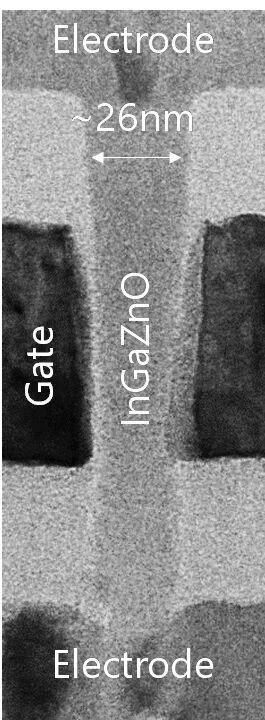
Cross-sectional TEM image of InGaZnO vertical transistors
InGaZnO transistors, due to their wide bandgap and high electron mobility, theoretically can achieve ultra-low leakage and high on-current simultaneously. Kioxia has experimentally achieved over 15μA of on-current while reaching ultra-low leakage below 10-18A by optimizing contact electrode materials and spacer thickness (as shown below). A significant portion of DRAM power consumption comes from refresh cycles. The lower the leakage, the longer the data retention time, diminishing refresh stress. Therefore, the core value of OCTRAM is to lower DRAM refresh power consumption with low-leakage oxide semiconductor transistors.
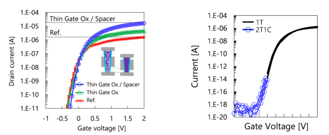
(a) On-current characteristics of the developed InGaZnO transistors and (b) off-current characteristics
In September 2025, Kioxia disclosed reliability studies related to OCTRAM, focusing on the TDDB lifetime issue of sub-25nm Gate-All-Around vertical InGaZnO transistors. TDDB stands for Time-Dependent Dielectric Breakdown, which refers to whether the transistor's insulating layer progressively deteriorates and ultimately fails under long-term electric field stress. Kioxia indicated that they found the deterioration in lifespan came from two factors: intrinsic factors brought by size scaling, and extrinsic factors due to manufacturing processes. By optimizing processes and reducing external degradation, Kioxia achieved an expected TDDB lifespan of over 10 years.
In December 2025, Kioxia announced closer core progress to 3D DRAM: the development of stackable oxide semiconductor channel transistors, achieving an 8-layer horizontal transistor stack with an on-current over 30μA, and an off-current below 1aA, equating to 10-18A.
As of now, Kioxia's 3D DRAM remains at the cutting-edge research and development stage and is not a commercial product yet.
Kioxia is not a traditional DRAM giant, but its accumulated stacking process, material integration, and array manufacturing capabilities from 3D NAND may provide it an entry point in the exploration of the next generation of 3D DRAM. Semiconductor Engineering also analyzes that Kioxia's 3D DRAM route borrows the mature oxide/nitride stacking capabilities in NAND to achieve lower-cost bit scaling, and then replaces channels with IGZO to reduce thermal degradation issues.
However, one point must be emphasized, Kioxia's 3D DRAM is not HBM. HBM is package-level 3D, stacking already manufactured DRAM dies to solve the high bandwidth issue next to the GPU. Kioxia's 3D DRAM is device/cell-level 3D, aiming to resolve the issue of DRAM cell scaling itself. Thus, Kioxia is not directly chasing HBM but exploring a more foundational 3D DRAM device route. If this path matures in the future, it could open new technical branches for large-capacity, low-power working memory in the AI era.
While 3D DRAM is still far from true commercialization, it currently resembles a technological ticket for the future rather than a product line immediately contributing to revenue. However, for Kioxia, the significance of this ticket is not small. In the short term, Kioxia can benefit from the NAND recovery driven by AI, pursue higher-level BiCS FLASH in the medium term, and long-term bet on 3D DRAM, transferring 3D stacking capabilities from NAND to DRAM.
Conclusion
From massive losses and merger stalemates to surpassing Toyota and topping Japan's market value in 2026, Kioxia's rollercoaster trajectory is almost filled with the cruel and charming tales of the semiconductor memory industry. It was once shunned by the capital market due to a singular product line and a missed opportunity in HBM, yet it has ushered in its golden era by adhering to NAND flash memory amidst the tsunami of “mass data flows” triggered by AI large models.
Kioxia's comeback may not yet indicate a true revival of the Japanese semiconductor industry. But it proves one thing: in the semiconductor industry, a downturn does not inevitably lead to exit. As long as technological assets remain, the rearrangement of cycles, capital, and demand can bring a forgotten company back to the center of the table at any moment.
For Kioxia, the next challenge of finding a sustainable balance between the fervent capital chase and the harsh industrial cycle will determine whether this sprout carrying the hope of Japan's semiconductor revival is merely a fleeting bloom in the AI super cycle or the beginning of a truly new storage empire.
*Disclaimer: This article is an original work by the author. The content of the article represents the author’s personal views, and Semiconductor Industry Observations reprints it solely to convey a different perspective, which does not represent Semiconductor Industry Observations' support or approval of the viewpoint. If there are any disputes, please feel free to contact Semiconductor Industry Observations.
免责声明:本文章仅代表作者个人观点,不代表本平台的立场和观点。本文章仅供信息分享,不构成对任何人的任何投资建议。用户与作者之间的任何争议,与本平台无关。如网页中刊载的文章或图片涉及侵权,请提供相关的权利证明和身份证明发送邮件到support@aicoin.com,本平台相关工作人员将会进行核查。


