Author: Godot
The two most popular sectors in AI are storage and optical technology. Previously, I wrote about the framework of storage (Understanding the profit pool and industrial pattern of AI storage layers in one article), and this article will focus on optical technology.
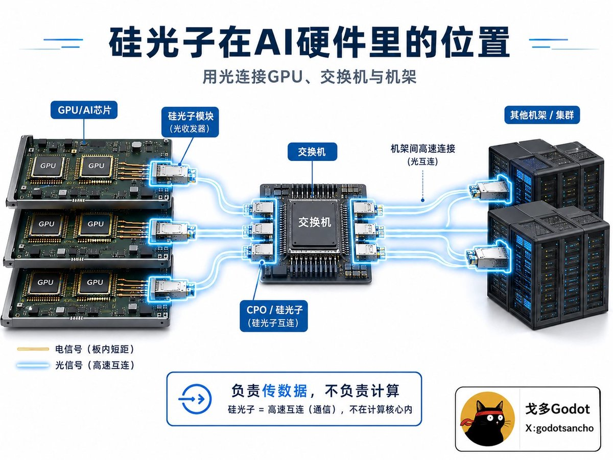
Silicon photonics is used for communication between computing chips, replacing the original copper wires, as illustrated in the image below.
Common terms you might encounter such as LPO (Linear Pluggable Optical), CPO (Co-Packaged Optics), OCS (Optical Circuit Switching), and Optical I/O refer to different technical routes for implementing silicon photonics.
Typically, chips communicate using copper wires. Silicon photonic chips incorporate lasers that can produce light, modulators that can "modulate" light, and *detectors that can "receive" light, directly onto the silicon substrate, utilizing photonic communication.
So, why replace copper? And why use silicon photonics instead of something else?
Firstly, copper wires nearly reach their physical limit when transmitting signals above 1.6T, leading to incomplete signals. There is a pressing need to consider alternative materials. This is the most critical issue, referred to as the bandwidth wall.
Secondly, copper is a tangible physical entity, and as GPU clusters increase in size, there is simply no room for more copper wires. This is another reason to replace copper. Light, on the other hand, can have optical interfaces directly soldered next to switch chips, saving considerable wiring. This is termed the scale wall.
Furthermore, copper consumes too much power. Silicon photonics can save tens of thousands of kilowatt-hours daily in hundreds of megawatt facilities, as this power is consumed in communication via copper wires. Once switched to light, this energy can be redirected for actual computations on GPUs. This is known as the power wall.
Interestingly, silicon photonics can leverage existing mature CMOS manufacturing processes in semiconductors, eliminating the need to build entirely new factories, allowing for low-cost mass production.
Of course, silicon photonics has a drawback; silicon itself cannot efficiently emit light and relies on indium phosphide (InP) materials. This has become a critical bottleneck in the entire industry chain.
The Evolution of Silicon Photonics Technology
The most significant milestone occurred in March 2025, when NVIDIA announced the Quantum-X and Spectrum-X photonic switches at the GTC conference. Jensen Huang declared that starting with the next generation of Rubin, "Optical interconnects are not optional, but standard."
One week later, NVIDIA announced an investment of $4 billion in Coherent and Lumentum to secure critical supply chains.
The silicon-based photoelectric effect was published in the 1980s, and between 2004 and 2014, Intel and IBM manufactured silicon-based optical modulators.
In the last decade, major cloud service providers like AWS, Google, and Meta applied silicon photonics, although at that time it was only a part of fiber optic communication.
Current Industry Landscape
1) The Bottom Layer: Wafer Foundries
Manufacturing photonic chips. TSMC $TSM leads with its COUPE process, while Tower Semiconductor $TSEM specializes in silicon photonics foundry, expecting a 70% year-over-year growth in silicon photonics revenue by 2025. GlobalFoundries $GFS became the largest dedicated silicon photonics foundry worldwide by acquiring Singapore's AMF.
2) The Second Layer: Core Component Suppliers
Providing lasers, modulators, etc. Mainly indium phosphide (InP) lasers, with fewer than five companies globally capable of producing high-speed EML lasers.
Lumentum $LITE is the only manufacturer that can mass-produce 200G/lane EML lasers, which are the core components of 1.6T optical modules. NVIDIA has already locked in orders with Lumentum until 2027.
3) The Third Layer: Module and System Manufacturers
Assembling components into products. Coherent holds 25% of the global optical transceiver market share. Chinese companies like Zhongji Xuchuang (InnoLight), Xinyi Sheng (Eoptolink), and Guangxun Technology (Accelink) are notable competitors in manufacturing scale and cost efficiency.
4) The Top Layer: System Integrators
NVIDIA, Cisco, Broadcom, and Marvell are all part of this layer.
In summary,
NVIDIA $NVDA
dominates the market, deciding which interconnect standards AI data centers adopt, and locking in supply chains through strategic investments.
Broadcom $AVGO
is an absolute leader in networking switching chips, holding nearly 80% of the Ethernet switch market. The Tomahawk 6-Davisson is the world's first 102.4 Tbps CPO switch.
Marvell $MRVL
is Broadcom's strongest challenger, dominating the PAM4 optical DSP market with a 60-70% share. Recently, it has acquired Celestial AI to enter the chip-to-chip optical interconnect space.
Lumentum $LITE
is the most critical supplier of EML lasers, being the only manufacturer globally capable of mass-producing 200G/lane EML lasers, and NVIDIA has locked in orders with them until 2027.
Coherent $COHR
is an integrator across the entire industry chain, with a layout that spans materials, lasers, and modules. FY2025 revenue estimates at $5.8 billion make it the top player in the optical transceiver market.
TSMC $TSM
is the process standard setter. The 65nm silicon photonics process is already in mass production, and the COUPE platform is currently the most advanced 3D heterogeneous integration scheme, deeply binding the NVIDIA CPO route.
Tower Semiconductor $TSEM
is the purest beneficiary of silicon photonics foundry. The revenue from silicon photonics is expected to grow 70% year-over-year by 2025, and they are investing $650 million to triple production capacity. Their market valuation elasticity is the strongest among all players.
Lightmatter / Ayar Labs Unlisted · IPO Candidates
Lightmatter is valued at $4.4 billion, focusing on 3D photonic interconnect; Ayar Labs received investments from AMD, Intel, and NVIDIA simultaneously, working on optical I/O chiplets. Both are potential heavy hitters for upcoming IPOs.
The Explosion of Silicon Photonics Brings a Change in Valuation Logic
For example, Wall Street previously valued Tower Semiconductor as a typical analog foundry, with a price-to-sales ratio of about 2-3 times.
However, when silicon photonics revenues grow from 5% to 30%-40% of total revenue, the market began to revalue them as rare assets in AI infrastructure, potentially raising the P/S ratio to 6-10 times.
Lumentum and Coherent were previously classified as telecom component suppliers; they are now redefined as essential providers of AI interconnects. BofA analyst Vivek Arya raised the target price for Marvell to $200, basing the logic on valuing Marvell as an AI infrastructure platform rather than a communication chip manufacturer.
Evercore ISI's judgment on Cisco is similar; as silicon photonics products penetrate large-scale data centers, Cisco's core AI revenue could explode to $12-15 billion from $3 billion over the next 3-4 years.
The Moat of the Silicon Photonics Industry
The silicon photonics industry shows a clear winner-takes-all characteristic, as each process has been developed over a long period prior to the AI explosion.
InP lasers: globally, fewer than five companies can mass-produce high-end EML lasers, with a production capacity expansion cycle of 3-5 years. This is the most bottlenecked segment in the entire industry chain.
TSMC's COUPE process: the process barrier of 3D heterogeneous integration requires competitors to lag by at least two generations and accumulate years of yield experience.
Foundry PDK ecosystems: once a client has designed at a particular foundry, switching costs are extremely high, requiring 12-18 months for redesign and re-certification.
Thermal management and packaging: CPO needs to effectively manage the coupling of electrical, thermal, and optical domains within a few millimeters. No viable products can be produced without several years of system integration experience.
Suppliers' certification processes for giants like AWS and Google typically take 12-24 months. Once certified, customer adhesion is incredibly strong.
Risks and Cold Reflections
The growth of the entire industry chain heavily relies on the capital expenditures of five large cloud firms: Microsoft, Google, Meta, Amazon, and Oracle.
There is potential substitutability in technology routes; LPO (Linear Pluggable Optical), CPO (Co-Packaged Optics), OCS (Optical Circuit Switching), and Optical I/O. If one route is disrupted by another, the capital invested previously may face depreciation and impairment.
Research institutions like LightCounting predict that significant large-scale CPO deployments will not emerge until after 2028; transitional solutions like LPO are expected to be in use before then.
Thus, betting on the overall industry victory is safer than betting on the success of a single company.
免责声明:本文章仅代表作者个人观点,不代表本平台的立场和观点。本文章仅供信息分享,不构成对任何人的任何投资建议。用户与作者之间的任何争议,与本平台无关。如网页中刊载的文章或图片涉及侵权,请提供相关的权利证明和身份证明发送邮件到support@aicoin.com,本平台相关工作人员将会进行核查。


