Original: He Lu Heng
Source: Far River Technology Review (ID: kechuangych)
After the release of NVIDIA's latest quarterly financial report, not only did AMD remain silent, but Intel also shed tears. Analysts who had been psychologically prepared for a long time did not expect the actual situation to exceed expectations to such an extent.
What's even more frightening is that NVIDIA's year-on-year revenue surged by 854%, largely because they "can only sell so much," rather than "selling so much." Behind a bunch of "start-up companies using H100 as collateral for loans" is the fact that there is a shortage of H100 GPUs.
If the shortage continues until the end of this year, NVIDIA's performance is likely to be even more shocking.
The shortage of H100 inevitably reminds people of a few years ago when GPU shortages due to the surge in cryptocurrency caused NVIDIA to be scolded by gamers. However, the shortage of graphics cards at that time was largely due to unreasonable markups, while the shortage of H100 is due to limited production capacity, and even with a price increase, it is still difficult to obtain.
In other words, NVIDIA is still making less money.
On the day the financial report was released, "production capacity" naturally became the most frequently mentioned term during the conference call. In response, NVIDIA spoke cautiously and refused to shoulder any blame that they shouldn't:
"In terms of market share, it is not something we can achieve alone, it requires many different suppliers."
In reality, when NVIDIA talks about "many different suppliers," it basically comes down to two:
SK Hynix and TSMC.
HBM: The Game of Koreans
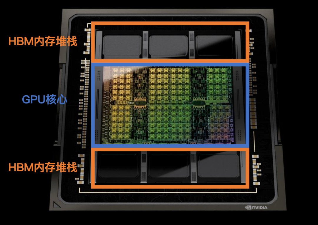
If we only look at the area ratio, a single H100 chip belongs to NVIDIA's part by only about 50%.
In the chip profile, the H100 die occupies the core position, with three HBM stacks on each side, adding up to an area equivalent to the H100 die.
These six ordinary memory chips are one of the culprits behind the shortage of H100 supply.
HBM (High Bandwidth Memory) is a type of memory in GPUs that handles part of the storage.
Unlike traditional DDR memory, HBM essentially stacks multiple DRAMs in the vertical direction, which increases memory capacity and effectively controls memory power consumption and chip area, reducing the space occupied inside the package.
"Stacked memory" was originally aimed at the smartphone market, which is very sensitive to chip area and heat. However, due to the high production cost, smartphones ultimately chose the more cost-effective LPDDR route, leaving stacked memory with no practical application.
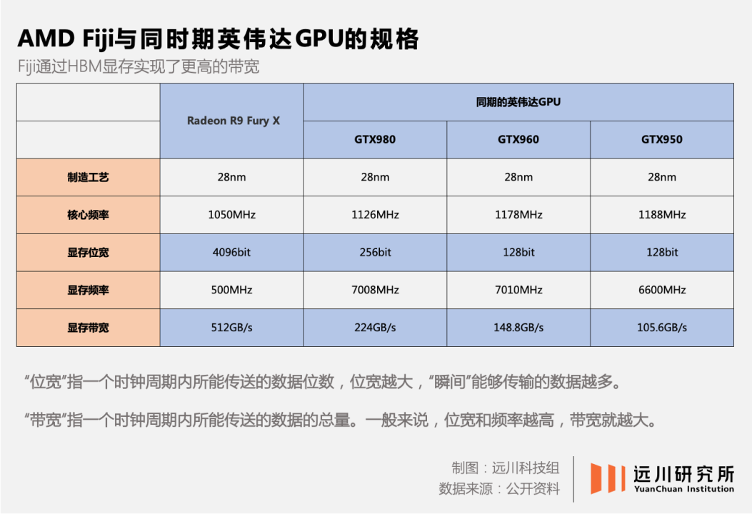
It wasn't until 2015 that AMD, whose market share was declining, hoped to follow in NVIDIA's footsteps with the popularity of 4K games.
In the AMD Fiji series GPU released that year, AMD used stacked memory developed in collaboration with SK Hynix and named it HBM (High Bandwidth Memory).
AMD's idea was that 4K games require greater data throughput efficiency, and the high bandwidth advantage of HBM memory could be demonstrated. At the time, AMD's Radeon R9 Fury X graphics card did indeed outperform NVIDIA's Kepler architecture new product on paper.
However, the bandwidth improvement brought by HBM was clearly unable to offset its high cost, so it did not become popular.
It wasn't until 2016, when AlphaGo swept the champion Go player Lee Sedol and deep learning emerged, that HBM memory suddenly found a use.
The core of deep learning lies in training models through massive data, determining parameters in functions, and incorporating actual data into decision-making to obtain the final solution.
In theory, the larger the amount of data, the more reliable the function parameters obtained, which makes AI training have an almost pathological pursuit of data throughput and data transmission latency, which is exactly what HBM memory solves.
In 2017, when AlphaGo played against Ke Jie again, the chip was replaced with Google's self-developed TPU. In chip design, every generation of TPU from the second generation onwards adopted HBM. NVIDIA's new GPU Tesla P100 for data centers and deep learning also used the second-generation HBM memory (HBM2).
With almost all high-performance computing GPUs equipped with HBM memory, the competition among storage giants around HBM quickly unfolded.
Currently, only three major memory manufacturers in the world can produce HBM: SK Hynix, Samsung Electronics, and Micron.
SK Hynix is one of the inventors of HBM and is the only manufacturer currently producing HBM3E (third-generation HBM). Samsung Electronics entered the market with HBM2 (second-generation HBM) and is the supplier of NVIDIA's first GPU using HBM. Micron is the most backward, only shifting from HMC to HBM in 2018 and starting mass production of HBM2 in mid-2020.
Among them, SK Hynix monopolizes 50% of the HBM market share, and its exclusive supply of HBM3E to NVIDIA firmly restricts the shipment volume of H100:
Both the H100 PCIe and SXM versions use 5 HBM stacks, the H100S SXM version can reach 6, and NVIDIA's promoted H100 NVL version even reaches 12. According to research institutions, the cost of a single 16GB HBM stack is as high as $240. So the cost of a single H100 NVL memory chip is close to $3000.
Cost is a small issue. Considering that Google's TPU v5 and AMD MI300, which directly compete with H100, will also use HBM3E, NVIDIA will be even more hard-pressed.
Faced with the surge in demand, it is said that SK Hynix has set a small goal to double its production capacity, and Samsung and Micron are also eager to use HBM3E. However, in the semiconductor industry, expanding production lines is never an overnight task.
Optimistically, it is estimated that it will take at least 9-12 months for HBM3E production capacity to be replenished, possibly not until the second quarter of next year.
Furthermore, even if the HBM production capacity issue is resolved, the amount of H100 that can be supplied still depends on TSMC's stance.
CoWoS: TSMC's Ace
Analyst Robert Castellano recently made a calculation. H100 is produced using TSMC's 4N process (5nm), and the price of a 12-inch wafer for the 4N process is $13,400, theoretically capable of cutting 86 H100 chips.
If we don't consider production yield, then for every H100 produced, TSMC can earn $155 in revenue.
However, in reality, the revenue brought by each H100 to TSMC is likely to exceed $1000, because H100 uses TSMC's CoWoS packaging technology, which brings in revenue as high as $723.
Every H100 that comes down from TSMC's N4/N5 production line at Fab 18 will be transported to TSMC's advanced packaging and testing Fab 2, also located in the same park, to complete the most special and crucial step in H100 manufacturing—CoWoS.
To understand the importance of CoWoS packaging, we still need to start with the chip design of H100.
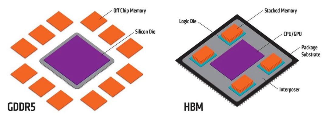
In consumer-grade GPU products, memory chips are generally packaged on the periphery of the GPU core, transmitting signals through circuits between PCB boards.
For example, in the RTX4090 chip, also from NVIDIA, the GPU core and GDDR memory are separately packaged and then assembled onto a PCB board, each independent of the other.
Both GPU and CPU follow the von Neumann architecture, which involves "separating storage and computation"—that is, when the chip processes data, it needs to retrieve data from external memory, and after the calculation is completed, transfer it back to memory, which causes a delay in computation. At the same time, the "quantity" of data transfer is also restricted.
The relationship between GPU and memory can be compared to Pudong and Puxi in Shanghai. The transportation of goods (data) between the two places relies on the Nanpu Bridge, and the carrying capacity of the Nanpu Bridge determines the efficiency of goods transportation, which is the memory bandwidth, determining the speed of data transfer and indirectly affecting the computing speed of the GPU.
From 1980 to 2000, the "speed mismatch" between GPU and memory increased at a rate of 50% per year. In other words, even if the Longyao Road Tunnel and Shangzhong Road Tunnel were repaired, they could not meet the increasing demand for goods transportation between Pudong and Puxi. This led to bandwidth becoming an increasingly obvious bottleneck in high-performance computing scenarios.
In 2015, while applying HBM memory, AMD also adopted an innovative solution for data transmission: combining Pudong and Puxi.
Simply put, the Fiji architecture graphics card in 2015 "sewed" HBM memory and GPU core together, turning several small chips into one large chip. This doubled the data throughput efficiency.
However, as mentioned earlier, due to cost and technical issues, AMD's Fiji architecture did not gain market acceptance. But with the explosion of deep learning and the relentless pursuit of data throughput efficiency in AI training, "chip stitching" found a use.
Additionally, while AMD's approach is good, it has also brought a new problem—no matter how many advantages HBM has, it must be combined with advanced "chip stitching" packaging technology, and the two are interdependent.
If HBM memory can be compared among different suppliers, it seems that only TSMC can provide the advanced packaging used for "chip stitching."
CoWoS is the starting point of TSMC's advanced packaging business, and NVIDIA is the first chip company to adopt this technology.
CoWoS is a combination of CoW and oS: CoW stands for Chip on Wafer, referring to the process of assembling the die on the wafer, and oS stands for on Substrate, referring to the process of packaging on the substrate.
Traditional packaging generally only involves the oS step, typically completed by a third-party testing and packaging factory after the wafer manufacturing is completed at the foundry. However, the additional CoW step in advanced packaging is not something that testing and packaging factories can handle.
Taking a complete H100 chip as an example, multiple HBM stacks are distributed around the H100 die, and they are stitched together using CoW technology. But it's not just about stitching; it also involves achieving communication between the die and the stacks.
TSMC's CoW differs from other advanced packaging in that it places the die and stacks on a silicon interposer (essentially a wafer), creating interconnect channels within the interposer to enable communication between the die and the stacks.
Similar to this is Intel's EMIB, which uses a silicon bridge for interconnect. However, the bandwidth is far less than that of the silicon interposer, and considering the close relationship between bandwidth and data transfer rate, CoWoS has become the only choice for H100.
This is another factor that is constraining H100 production capacity.
Although CoWoS has incredible effects, the sky-high price of $4000-6000 per chip has deterred many, including the wealthy Apple. Therefore, TSMC's prepared production capacity is quite limited.
However, the sudden surge in demand due to the AI wave has disrupted the supply-demand balance.
Rumors in June suggested that NVIDIA's demand for CoWoS this year had reached 45,000 wafers, while TSMC's initial estimate at the beginning of the year was 30,000 wafers. With the additional demand from other customers, the production capacity shortfall exceeded 20%.
To make up for the shortfall, TSMC has made significant efforts.
In June, TSMC officially launched its advanced packaging Fab 6 in the same South Science Park, with a clean room larger than all other packaging factories combined, and promised to increase CoWoS production capacity seasonally, outsourcing some oS to third-party packaging factories.
However, just like the difficulty of expanding HBM production, expanding TSMC's production also takes time. Currently, the delivery time for some packaging equipment and components ranges from 3 to 6 months, and it is still unknown how much new capacity can be opened up by the end of the year.
Non-existent Plan B
Faced with the structural shortage of H100, NVIDIA does not completely lack a Plan B.
During the conference call after the financial report was released, NVIDIA revealed that other suppliers have been involved in certifying CoWoS production capacity. Although they did not specify who, considering the technological barriers to advanced packaging, apart from TSMC, only Intel's EMIB, which has inherent shortcomings, and Samsung's I-Cube, which has been developed for a long time but has not attracted customers, could barely come to the rescue.
But changing core technology is like changing generals before a battle. With the imminent mass production and shipment of AMD MI300, the competition in AI chip technology is heating up. Whether it can be compatible with Intel and Samsung's technology, Huang Renxun himself is probably also anxious.
The ones who might be more anxious than Huang Renxun are the cloud service providers and AI startups that cannot buy H100. After all, if gamers can't get graphics cards, it just means a loss of 20 frames per second in games; if large companies can't get H100, they may lose tens of billions in revenue and hundreds of billions in valuation.
The companies that need H100 mainly fall into three categories: cloud service providers like Microsoft and Amazon; startups like Anthropic and OpenAI; and large tech companies like Tesla, whose new FSD solution uses a GPU cluster composed of 10,000 H100 chips for training.
This doesn't even include financial companies like Citadel, and Chinese companies that can't buy the special edition H800.
According to GPU Utils' calculations, the conservative estimate is that the supply gap for H100 has reached 430,000 units.
Although there are theoretical alternative solutions to H100, they lack feasibility in practice.
For example, the predecessor of H100, the A100, is only about 1/3 of the price of H100. However, the problem is that the performance of H100 is much stronger than A100, resulting in a higher cost-effectiveness of H100 per unit. Considering that tech companies purchase hundreds or thousands of units, buying A100 would actually be more of a loss.
AMD is another alternative, and its performance on paper is not much different from H100. But due to the barriers of NVIDIA's CUDA ecosystem, using AMD's GPU is likely to lengthen the development cycle, and the competitors using H100 may pull ahead due to this time difference, even leading to a total loss of investment of hundreds of millions of dollars.
For various reasons, a chip with a total material cost of $3000, NVIDIA is selling it with an extra zero, and everyone is actually rushing to buy it. This may be something that even Huang Renxun himself did not expect.
And before the improvement of HBM and CoWoS production capacity, the only way to buy H100 might be:
Wait for those startups that bluffed their way into money to buy a bunch of H100 to go bankrupt, and then take over their second-hand GPUs.
Reference materials
[1] AI Capacity Constraints - CoWoS and HBM Supply Chain, SemiAnalysis
[2] Original factory actively expanding production, estimated annual growth rate of HBM bits supply in 2024 is 105%, TrendForce
[3] How will HBM technology change data centers? Semiconductor Industry Vertical and Horizontal
[4] Advanced Packaging Part 2: Intel, TSMC, Samsung, AMD, UMC, Sony, Micron, SK Hynix, YMTC, Tesla, and NVIDIA's Options/Usage Review, Semianalysis
[5] OpenAI co-founder and part-time scientist Andrej Karpathy's tweet
[6] Taiwan Semiconductor: Significantly Undervalued As Chip And Package Supplier To Nvidia, SeekingAlpha
[7] Nvidia H100 GPUs: Supply and Demand, GPU Utils
Editor: Li Motian
Visual Design: Shu Rui
Responsible Editor: Li Motian
免责声明:本文章仅代表作者个人观点,不代表本平台的立场和观点。本文章仅供信息分享,不构成对任何人的任何投资建议。用户与作者之间的任何争议,与本平台无关。如网页中刊载的文章或图片涉及侵权,请提供相关的权利证明和身份证明发送邮件到support@aicoin.com,本平台相关工作人员将会进行核查。


