Original Source: TMT Post
Author: Lin Zhijia
Image Source: Generated by Wujie AI
NVIDIA DGX H200, which was released just over half a year ago, once again caused a sensation late at night today.
TMT Post App learned that on the evening of November 13th, Beijing time, the American chip giant NVIDIA released the world's most powerful AI chip - NVIDIA H200 Tensor Core GPU (graphics processor).
The new NVIDIA H200 is an upgraded product of the current H100, based on the NVIDIA Hopper super chip architecture, with the highest performance and advanced memory technology features, designed for ultra-large-scale large model training and inference, and can enhance generative AI and high-performance computing (HPC) workloads.
H200 is the first GPU product to offer a speed of 4.8 TB per second and 141GB of HBM3e memory. Compared to H100, H200 has almost doubled the capacity and increased bandwidth by 2.4 times. When used for large model inference or generation problems such as Llama2 and GPT-3, the performance of H200 is 60% to 90% higher than H100 (1.6-1.9 times). Therefore, H200 can be deployed in various types of data centers, including on-premises, cloud, hybrid cloud, and edge.
Furthermore, compared to the CPU (central processing unit), the results speed obtained by H200 in HPC is "terrifying": increased by 110 times.
For the Chinese market, on the morning of November 14th, NVIDIA confirmed to TMT Post App in an email: Without an export license, H200 will not be able to be sold in the Chinese market.
It is understood that NVIDIA H200 will begin to supply to global customers and cloud service providers in the second quarter of 2024, and is expected to compete with AMD's MI300X AI chip.
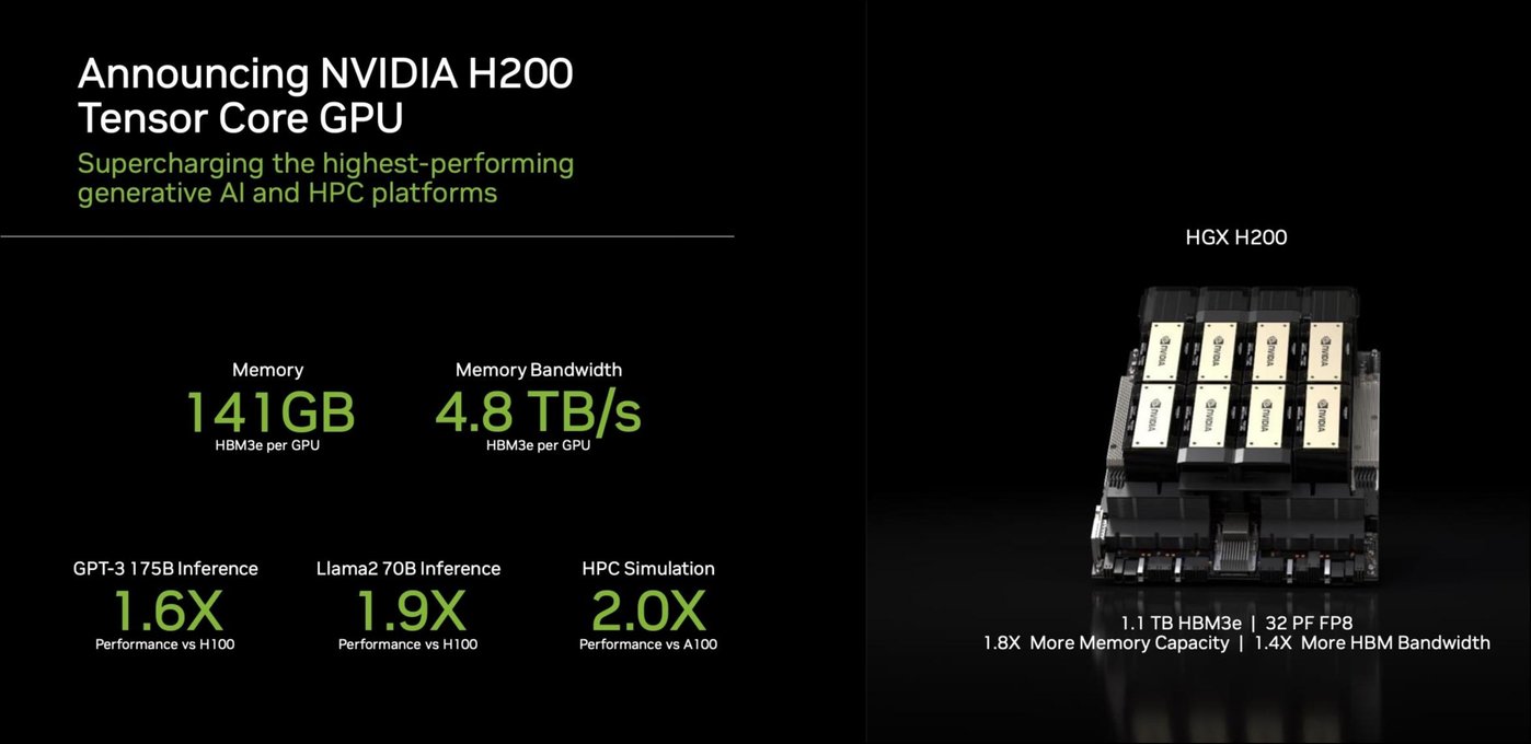
NVIDIA HGX H200 processor (Source: NVIDIA official website)
Specifically, with the support of NVIDIA Hopper architecture, TensorRT-LLM dedicated software, and other hardware and software technologies, the new H200 demonstrates excellent performance in ultra-large model training and inference. Compared to H100, H200's inference speed for the open-source large model Llama 2 (700 billion parameters) is almost doubled, and future software updates are expected to bring additional performance advantages and improvements to H200.
According to NVIDIA data, in TF32 Tensor Core, H200 can achieve 9.89 trillion floating-point operations; under INT8 tensor core, it provides 3,958 TFLOPS (3.958 trillion floating-point operations per second).
Moreover, the HGX H200 acceleration server platform built on the H200 chip has high-speed interconnection support with NVLink and NVSwitch. Eight HGX H200s provide over 32 petaflops of FP8 deep learning computing and 1.1TB aggregated high-bandwidth memory, providing higher performance support for workloads such as scientific research and AI applications, including training and inference of models with over 175 billion parameters.
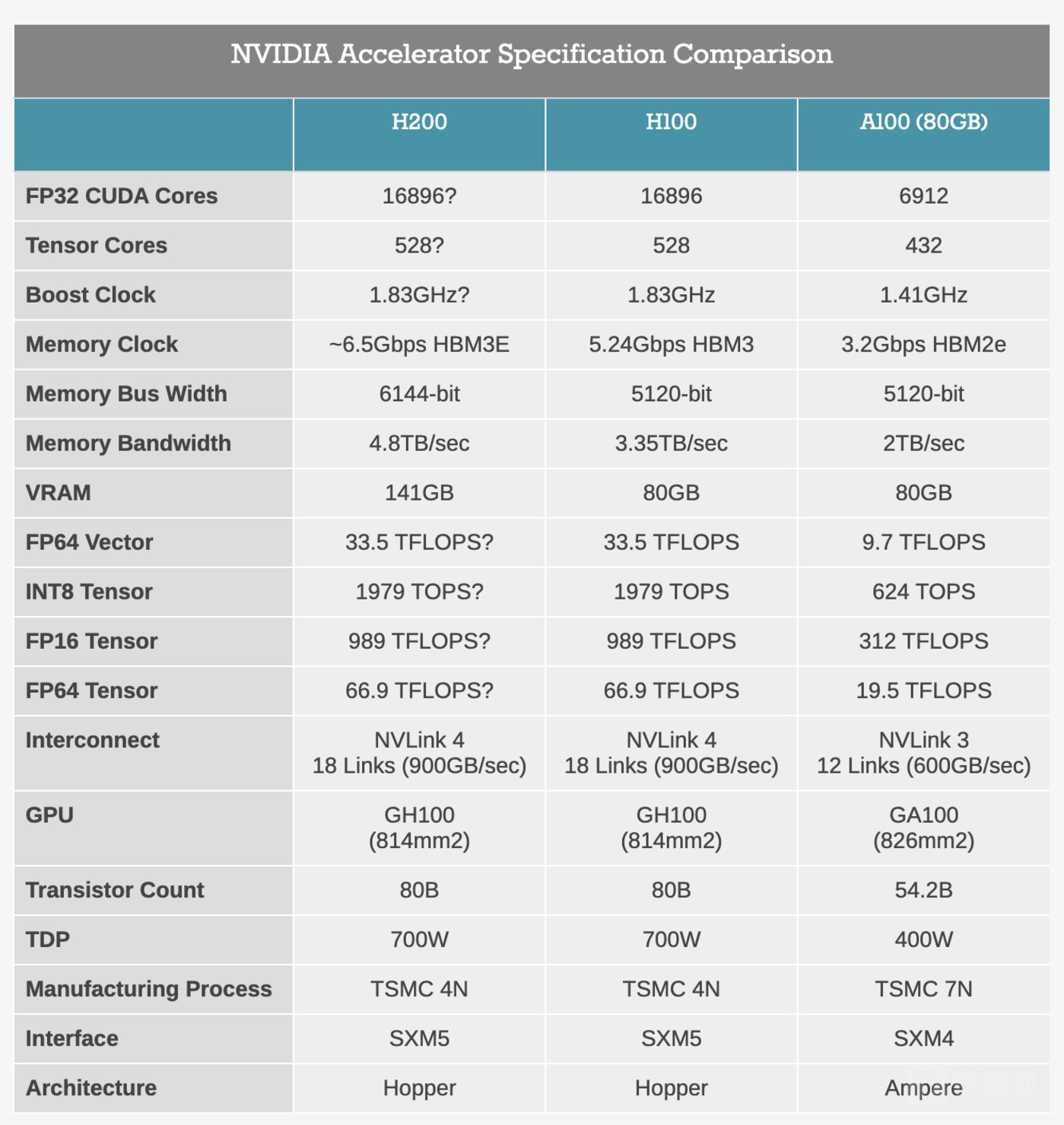
Performance specifications comparison of NVIDIA H200, H100, and A100 (Source: anandtech)
According to Anandtech's analysis, based on the current specifications, the accelerated computing performance of H200 can be understood as half of the GH200 Hopper super chip released six months ago, with the difference being that HBM3 is replaced by HBM3e, the memory bandwidth is increased from 80GB to 141GB, and the speed is increased to 4.8TB/s, allowing NVIDIA to improve the processing speed and bandwidth capacity. Based on the total bandwidth and memory bus width, the memory frequency of H200 is approximately 25% higher than that of H100.
TMT Post App confirmed with NVIDIA that if there is no export license, the new H200 will not be sold to China, because the parameters of H200 exceed the performance red line announced by the U.S. Department of Commerce on October 17th: the total processing performance of multiple digital processing units (used for data centers) is 2400-4800, with a "performance density" greater than 1.6 and less than 5.92.
In early November, NVIDIA has announced "China Special Edition" HGX H20, L20 PCle, and L2 PCle products to distributors, targeting training, inference, and edge scenarios, which will be announced as early as November 16th, with mass production scheduled for December 2023 to January 2024. Among them, HGX H20 has limitations in bandwidth, computing speed, and other aspects, with a theoretical comprehensive computing power about 80% lower than NVIDIA H100, and of course, it will be more "shrunk" than H200.
It is worth mentioning that, in addition to H200, based on NVIDIA's current AI chips based on Grace, Hopper, and Grace Hopper architectures, the company today launched a new platform with 4 Grace Hopper GH200 AI chips, called NVIDIA Quad GH200.
Quad GH200 provides 288 Arm CPU cores and a total of 2.3TB of high-speed memory. By stacking four GH200s, with 8 chips and 4-way NVLink topology interconnected, it forms a powerful computing platform jointly supported by CPU and GPU, providing more user-friendly and powerful computing power support when installed in infrastructure systems.
According to the U.S. financial institution Raymond James, the cost of the H100 chip is only $3,320, but NVIDIA's batch price to its customers is still as high as $25,000 to $40,000, resulting in a profit margin of up to 1000%, making it the most profitable chip in history.
According to the NVIDIA official website, NVIDIA H200 will support over 40 AI supercomputers. Companies including CoreWeave, Amazon AWS, Google Cloud, Microsoft Azure, and Oracle Cloud will be the first to deploy cloud service providers based on H200 instances. In addition, system integrators such as ASUS, Dell Technologies, HP, Lenovo, Supermicro, and Wistron will also use H200 to update their existing systems.
Furthermore, NVIDIA also hinted on its official website that the upcoming NVIDIA B100 AI chip will have a larger performance upgrade next year. "The NVIDIA Hopper architecture has achieved unprecedented performance leaps."
免责声明:本文章仅代表作者个人观点,不代表本平台的立场和观点。本文章仅供信息分享,不构成对任何人的任何投资建议。用户与作者之间的任何争议,与本平台无关。如网页中刊载的文章或图片涉及侵权,请提供相关的权利证明和身份证明发送邮件到support@aicoin.com,本平台相关工作人员将会进行核查。


