Really have to thank today's Huawei's Tao (τ) law, which saved the big A!
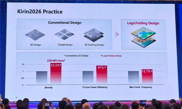
This might be another #Deepseek moment, the essential logic is very simple: we are constrained by advanced lithography machines and process technology in terms of chip size, so we take a different approach, not reducing size but instead reducing time.
By using 3D stacking technology, we make the signal run a bit faster to achieve the same performance. This has achieved the effect equivalent to 5 nanometers and 3 nanometers on mature chip processes of 14 nanometers and 7 nanometers. This solution is now fully commercially used by Huawei in 381 chip models.
No wonder today domestic chip concept stocks surged across the board. The US stock market is hyping optical modules, MLCC, and 800V DC architecture. The A-share market now has a new direction with 3D packaging, hybrid bonding, and thermal management, all surging today. I'm still holding onto GigaDevice Innovation, waiting for Changxin's IPO, and am optimistic about Zhu Yiming! 🧐
Trading stocks really is the best driving force for learning, with a bunch of new concepts recently, which not only requires brain power but also quite a lot of AI tokens. 😂
免责声明:本文章仅代表作者个人观点,不代表本平台的立场和观点。本文章仅供信息分享,不构成对任何人的任何投资建议。用户与作者之间的任何争议,与本平台无关。如网页中刊载的文章或图片涉及侵权,请提供相关的权利证明和身份证明发送邮件到support@aicoin.com,本平台相关工作人员将会进行核查。


