Source: Silicon Alien

Image source: Generated by Wujie AI
In fact, when NVIDIA announced the launch of the H200 Tensor Core GPU on November 13th, it didn't come as a surprise.
After all, on August 30th, NVIDIA released the news that its GH200 Grace Hopper would be equipped with HBM3e, with the aim of giving the next generation of Tensor Core GPU products an absolute performance advantage. But when Huang Renxun stood on the stage and loudly recited the detailed parameters of the H200 on the screen, there was nothing left but exaggeration.
To briefly go over the parameters, the H200's memory is 141GB, with a bandwidth of 4.8TB per second. Because the version released this time is the SXM version, which comes with a high-bandwidth socket. So compared to the SXM version of the H100, the memory has increased by 76% from 80GB, and the bandwidth has increased by 43% from 3.35TB per second. But that's not the main point. Whether it's the H100 or H200, they both focus on complex artificial intelligence calculations, so in terms of business, the inference speed of the Llama2 700 billion parameter model has increased by 90%, and the inference speed of the GPT-3 175 billion parameter model has increased by 60%.
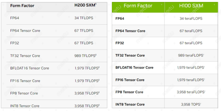
This makes people curious, because in terms of floating point calculation capability, the larger the number, the more powerful it is. But from the panel perspective, for the SXM versions of both H100 and H200, regardless of FP64 or other precisions, they are completely the same. It's worth noting that the entire floating point precision of the single PCIe version of the H100 is lower than that of the SXM version, so its bandwidth is only 2TB per second, while the SXM version of the H100 mentioned earlier has 3.35TB per second. The difference in floating point precision will bring about performance differences, so how can there be differences between two cards with the same precision?
Left: H200, Right: H100
Internal strength is called HBM3e
This is like the old man in martial arts novels who looks weak but can easily knock down a strong man with a single move, this is "internal strength." The H200 this time uses the same hopper architecture as the H100, with the biggest difference being the use of the aforementioned HBM3e. Let's break down these English letters. HBM stands for High Bandwidth Memory, which is a memory interface built using three-dimensional stacked dynamic random access memory (SDRAM) technology, which refers to the use of the vertical concept to expand memory while significantly increasing stack internal processing speed. In simple terms, in the past, everyone lined up in a single file inside the memory, and the first one had to finish processing before the next one could come in, not utilizing space, just utilizing the plane. But with HBM, multiple windows are set up, but they are established vertically, making the queue speed faster.
On the other hand, compared to dynamic random access memory, also known as DRAM, and SDRAM, SDRAM adds synchronous and dual-bank functionality to the architecture of DRAM, allowing the microprocessor to synchronize with the clock of SDRAM, so SDRAM can save more time when executing commands and transferring data compared to DRAM. With the increase in queue windows, the queue speed also increases, so the overall efficiency naturally increases. Finally, with 3e, 3 represents the third generation architecture, and e represents the enhanced version of the third generation architecture, similar to a DLC in a game.
NVIDIA's H100 uses HBM3 produced by SK Hynix in June 2022 (the PCIe version of the H100 uses HBM2e, just to clarify), with a stack memory bandwidth of 819GB per second. HBM3e is an upgrade to HBM3 within the same architecture, with upgrades to materials, logic, and algorithms, and the memory bandwidth has been increased by a significant 25% to 1TB per second. So going back to the initial question, the operation of the Llama2 model generally follows the principle of consuming 3 to 5GB of memory for every 10 billion parameters, but this can decrease with version updates and algorithm optimizations, as developers also aim to prevent memory overflow and unforeseen errors. In other words, the larger the memory, the faster the operation efficiency.
But it's only a 25% increase! Don't worry, NVIDIA's bold move is still to come. It's said that internal training is important, but don't forget, external training is also crucial. Both the H200 and H100 use the Hopper architecture, but NVIDIA has "armed" the former with TensorRT-LLM. NVIDIA's TensorRT-LLM consists of the TensorRT deep learning compiler, including optimized kernels, preprocessing and post-processing steps, and multi-GPU/multi-node communication primitives.
External strength is called TensorRT-LLM
The working principle of TensorRT-LLM is similar to the story of "Gauss's sum." While other kids are still adding up arithmetic series one by one, Gauss quickly comes up with a formula to calculate the result. TensorRT-LLM is like such a formula, helping the GPU quickly solve complex calculations through software optimization. Taking the H100 as an example, after using TensorRT-LLM, the efficiency of the H100 in summarizing articles on some media websites is twice as fast as before. And on the Llama2 with 700 billion parameters, the former is 77% faster than the latter. NVIDIA played a trick, as on the official comparison, the H200 SXM is compared to the H100 SXM without using TensorRT-LLM. Of course, this is another story, as TensorRT-LLM is not intended for the H100. In summary, with HBM3e on the internal side and TensorRT-LLM on the external side, NVIDIA can achieve such a significant performance improvement over the previous generation products without changes in computational precision.
At the beginning of 2023, NVIDIA's closing price was around 140, and after the release of the H200, as of the time of writing, the closing price is 489, an increase of 230% from the beginning of the year. Alright, this time, Huang has gone completely crazy, and if I were him, I'd probably be even crazier. But hold on, in June of this year, a long-time rival of NVIDIA, Huang Renxun's cousin's granddaughter, Su Zifeng, also known as Huang Renxun's grandniece, stepped forward. She brought out an AMD GPU, the MI300X, to challenge the position of the H200.

Su Zifeng with the MI300X
Despite still using HBM3 memory, AMD has come up with a "more for the same price" move, as the memory of the MI300X has reached 191GB, a full 35% higher than the H200. What does 191GB mean in a GPU? The H100 has a version called the H100 NVL, which is very straightforward. It uses two PCIe versions of the H100 directly soldered together, resulting in an effect where 1+1 > 2, which also brings the memory to 188GB. However, big also has its downsides. The rated power of the MI300X is 750W, 50W more than the H200. Unlike memory, power is the opposite, the lower the rated power, the lower the maintenance cost and the more durable the device. Generally, artificial intelligence labs do not use just one GPU product, they mostly make multiple purchases, so if each MI300X consumes 50W more power than the H200, it could ultimately lead to a loss of competitiveness.
For NVIDIA, there is also a headache. Several Chinese internet giants have been loyal customers of the A100 and H100, but the United States quickly banned the sale of these two GPU products to China. To make matters worse, with the ban issued by the United States in October 2023, the Chinese custom versions of the A100 and H100, the A800 and H800, will also be banned from sale to China after November 17th. Looking at the financial reports, NVIDIA's data center receives about 25% of its revenue from China, so it's likely that the H200 will soon be listed as one of the products prohibited from being sold to China.
免责声明:本文章仅代表作者个人观点,不代表本平台的立场和观点。本文章仅供信息分享,不构成对任何人的任何投资建议。用户与作者之间的任何争议,与本平台无关。如网页中刊载的文章或图片涉及侵权,请提供相关的权利证明和身份证明发送邮件到support@aicoin.com,本平台相关工作人员将会进行核查。


